 |
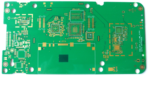
层数/Layers:12Layers FR4 板厚/Thickness: 2mm 最小孔径/Min.Laser Via Size: 0.10mm 线宽线距/Width/Spacing:3.5/3.5mil 表面处理/Surface Treatment : ENIG 特殊工艺/Special Process: HDI 1+1+N+1+1, Resin Filling+Plating Pluged 应用领域/Appilcation:Communication equipment |
HDI PCB
HDI PCB also calls High Density Interconnector PCB or HDI Technology , HDI circuit board is defined as a PCB with a higher wiring density with finer trace and spacing per unit area than normal PCB. They have finer lines and spaces, smaller via holes and solder pads and higher connection pads density than the conventional PCB (Quick turn PCB) design technology. HDI PCB is normally used to reduce PCB size and weight, as well as to improve electrical performance of the device. HDI PCB is the best alternative to high layer PCB, or small size PCB without enough design space.

